Enabling Miniaturization with Micro 3D Printing
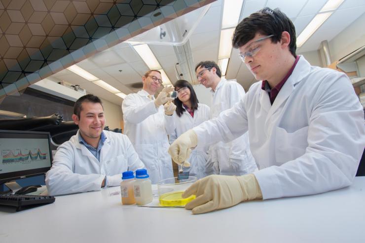
The trend of miniaturization is gaining momentum, as the demand for smaller and smaller parts for consumer electronics, medical devices, robotics, and life sciences grows. One of the new frontiers in Additive Manufacturing (AM) is the production of high-resolution, high-accuracy microstructures for industrial applications. These parts are not only difficult to prototype using existing 3D printers, but they are also often much more expensive and complicated to manufacture.
Ougazzaden and Collaborators Awarded ANR Grant for Optically Stimulated Cochlear Implants
Sep 30, 2022 — Metz, France

Schematic of CORTIORGAN flexible optical implant in cochlea with individually addressed blue LEDs spaced 60 𝜇m from each other (not all LEDs shown). Cross-section cut-outs in schematic show path of implant inside cochlea.
For individuals suffering from hearing loss, good news may be on the horizon thanks to cutting-edge optical technology. The French National Research Agency (ANR) has awarded Abdallah Ougazzaden, professor of Electrical and Computer Engineering at Georgia Tech and president of Georgia Tech-Lorraine, a €560,000 ($560,700) grant to develop technology for a new class of cochlear implants that may be able to restore hearing for patients.
The project aims to create optically stimulated, reduced-size, high-density cochlear implants with removable LEDs (CORTIORGAN). Project collaborators include Jean-Paul Salvestrini, director of the Georgia Tech-CNRS IRL 2958 lab and adjunct lecturer in the School of Electrical and Computer Engineering (ECE); Paul Voss, associate professor in ECE; and Suresh Sundaram, adjunct lecturer in ECE.
“CORTIORGAN is taking the technology for cochlear implants in a completely new direction through the optical stimulation of the cochlea with compact, dense, and highly flexible LED implants,” Ougazzaden said. “In particular, we will use a new semiconductor material – a two-dimensional hexagonal boron nitride – that brings about a radical rethinking of existing methods for processing inorganic LED devices.”
The key technology is based on optogenetics, a groundbreaking biological technique that stimulates neurons and other cells with light. The technology has a range of medical and neuroscience applications, including sight recovery and blocking pain signals.
The researchers will use optogenetic methods to achieve optical stimulation of auditory nerves rather than traditional electrical stimulation. Because tissue inside the cochlea has high electrical conductivity, optical stimulation of nerves can result in better spatial resolution and thus better implants.
CORTIORGAN’s goal is to develop removable ultra-thin LEDs that can be packaged in cochlear implants. The novel process allows the researchers to achieve size and flexibility requirements for cochlear implants that will be inserted into mouse cochlea and tested at the end of the project.
“This innovation will have a strong positive impact on the hearing-impaired by offering them an optical implant with greater spatial resolution and higher sound reproduction fidelity in comparison to existing electrical stimulation technology,” Ougazzaden added. “This optical technology will open the door for future neuroscience applications with many opportunities for commercialization.”
Other partners include Institut Pasteur, a renowned Paris-based center for biomedical research, and the Center for Nanosciences and Nanotechnologies (C2N), a collaboration between the University of Paris-Saclay and the French National Center for Scientific Research (CNRS).
Writer: Catherine Barzler, Senior Research Writer/Editor
Image: Georgia-Tech Lorraine
Andrea Gappell, Communications Manager, Georgia Tech-Lorraine
Partnership with DOD’s Microelectronics Work¬force Development Program Continues, Expands
Sep 27, 2022 — Atlanta, GA

The nearly $11M, five-year extension of the SCALE program aims to restore global lead through education initiatives.
The Scalable Asymmetric Lifecycle Engagement Microelectronics Workforce Development program (SCALE) has announced the program will extend another five years and expand with $10.8 million additional Department of Defense (DoD) funding, with a ceiling of $99 million.
SCALE officials said this expansion of the nation’s preeminent program will further its goal to develop a next-generation workforce that can return the United States to prominence in global microelectronics manufacturing.
Georgia Tech participates in the partnership, which is led by Purdue University and managed by NSWC Crane. SCALE facilitates the training of highly skilled U.S. microelectronics engineers, hardware designers and manufacturing experts. SCALE brings together a public-private-academic partnership of 17 universities and 34 partners within the defense industry and government.
“This is an extremely exciting time in the country and at Tech for microchip design and manufacturing,” said Arijit Raychowdhury, the Steve W. Chaddick School Chair of Tech’s School of Electrical and Computer Engineering (ECE). “These newly announced funds for the SCALE program will help Georgia Tech recruit a new, diverse group of students ready to work in defense microelectronics. We’re thrilled to be a SCALE partner university and honored to be leading many of the project’s specialty areas.”
SCALE provides unique courses, mentoring, internship matching and targeted research projects for college students interested in five microelectronics specialty areas. Georgia Tech ECE faculty members will be the primary investigators for three of the areas:
- system on a chip will be led by Raychowdhury;
- radiation-hardening will be led by John Cressler;
- and heterogeneous integration/advanced packaging will be led by Madhavan Swaminathan.
The other two focus areas are embedded system security/trusted AI and supply chain awareness.
Industry and government partners regularly meet and update a list of knowledge, skills, and abilities important for new entrants to the workforce. The SCALE universities then update their curriculum to ensure the students are prepared for upcoming needs in the rapidly advancing microelectronics field.
Peter Bermel, SCALE director and the Elmore Associate Professor of Electrical and Computer Engineering at Purdue, said the United States will need 50,000 trained semiconductor engineers to meet overwhelming and rapidly growing demand.
“The United States is committed to expanding and strengthening its semiconductor industry and workforce rapidly over the next five years,” Bermel said. “SCALE takes a holistic approach to the microelectronics workforce gap by comprehensively addressing system challenges for workforce training and recruiting.”
Goals for the next five years include:
- Expanding student participation in SCALE fivefold to more than 1,000.
- Developing learning models for K-12 classrooms.
- Collaborating with community colleges nationwide to develop microelectronics classes.
The demand for microelectronics increased by 26.2% in 2021. But while the United States consumes about half of the chips produced worldwide, the country only manufactures about 12%, highlighting the pressing need for the U.S. to bolster its domestic semiconductor supply chains and industrial capacity.
The funding announcement is the latest highlight in Georgia Tech’s leadership role in bolstering microelectronics and workforce development. Tech’s large engineering and science faculty bring a broad set of research expertise to strengthen the country’s semiconductor capacity. The Institute is uniquely positioned to train the microelectronics workforce, drive future microelectronics advances, and provide fabrication and packaging facilities for industry, academic and government partners to develop and test new solutions.
Dan Watson
dwatson@ece.gatech.edu
Resonances for Spatially Distributed Emitters
Georgia Electronic Design Center Distinguished Lecture Series
Resonances for Spatially Distributed Emitters
Featuring Steven Johnson, Professor of Applied Mathematics and Physics, MIT
Electromagnetics for Next-Generation Body Area Sensing
Georgia Electronic Design Center Distinguished Lecture Series
Electromagnetics for Next-Generation Body Area Sensing
Featuring Asimina Kiourti, Associate Professor, Electrical and Computer Engineering The Ohio State University
Abstract: Rapid advances in bio-electromagnetics are opening new and unexplored opportunities in body area sensing, empowering the vision of roundthe-clock monitoring “in the wild”.
Biocleanroom Open House
Join us for the Georgia Tech Biocleanroom's first open house on October 27th at 10:00 a.m. Attendees will learn more about the tools available, meet the biocleanroom staff, and tour the lab facility. There will also be a free training session on the FTIR and Q600 as well as a demo on the Nanoscribe.
Free coffee and pastries will be provided for attendees.
Please register by October 25th.
Zandehshahvar Awarded SPIE Optics and Photonics Education Scholarship
Sep 22, 2022 — Atlanta, GA
Mohammadreza (Reza) Zandehshahvar has been awarded a 2022 Optics and Photonics Education Scholarship by SPIE, the international society for optics and photonics, in recognition of his research on machine learning for inverse design and knowledge discovery in nanophotonics.
Reza is a Ph.D. candidate in the Georgia Tech School of Electrical and Computer Engineering (ECE). He has been a member of ECE’s Photonics Research Group, directed by Ali Adibi, the Professor and Joseph M. Pettit Chair in Electronics and Nanophotonics, since 2018.
His current research focuses on developing unsupervised learning models for knowledge discovery in nanophotonics. Other research interests include medical image processing, active learning, and metric learning.
According to SPIE, the key criterion in evaluating and ranking applications for the scholarship is the "prospect for long-term contribution that the granting of an award will make to the field of optics, photonics or related field." This year SPIE has award $293,000 in education scholarships to 78 outstanding SPIE Student Members, based on their potential contribution to optics and photonics, or a related discipline. Award-winning applicants were evaluated, selected, and approved by the SPIE Scholarship Committee. Through 2021, SPIE has distributed over $6 million in individual scholarships.
Earlier this year, Zandehshahvar was awarded the ECE Faculty Award at the School’s annual Roger P. Webb Awards Program. The award is given annually to the electrical or computer engineering student who, in the opinion of the ECE faculty, has done the most to improve the educational environment within ECE or Georgia Tech, and has contributed significantly to both student welfare and student-faculty interactions.
Additionally, he received the 2022 VIP Outstanding Mentor Award for mentoring students on the projects related to machine learning for inverse design in nanophotonics and medical image processing for diagnosis and prognosis of lung diseases. Georgia Tech’s Vertically Integrated Projects (VIP) program is a transformative approach to enhancing higher education by engaging undergraduate and graduate students in ambitious, long-term, large-scale, multidisciplinary project teams that are led by faculty. Reza is the lead mentor on the AI-based Discovery and Innovation VIP team since 2019.
Dan Watson
dwatson@ece.gatech.edu
Fall 2022 IEN Microfabrication Short Course
IEN Microfabrication Short Course
The Institute for Electronics and Nanotechnology (IEN) at Georgia Tech will offer a short course on microfabrication from November 3rd - 4th, 2022. This intensive two-day short course combines classroom lectures and laboratory based hands-on fabrication in the IEN cleanroom. The goal of the course is to impart a basic understanding of the science and technology of microfabrication processes as used in academia and industry.
Microchip Can Electronically Detect Covid Antibodies in Just a Drop of Blood
Sep 21, 2022 — Atlanta, GA

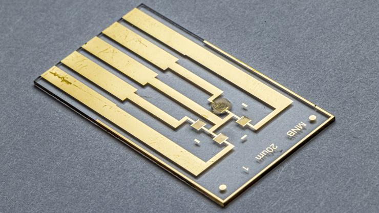
A custom microchip that detects Covid-19 infection electronically and can differentiate between vaccine-induced antibodies and those created as a result of a coronavirus infection. (Photo: Candler Hobbs)
A single drop of blood from a finger prick. A simple electronic chip. And a smartphone readout of test results that could diagnose a Covid-19 infections or others like HIV or Lyme disease.
It sounds a bit like science fiction, like the beginnings of the medical tricorder used by doctors on Star Trek. Yet researchers at Georgia Tech and Emory University have taken the first step to showing it can be done, and they’ve published their results in the journal Small.
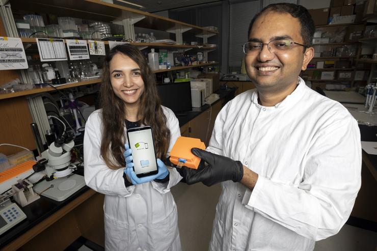
Postdoctoral fellow Neda Rafat and Assistant Professor Aniruddh Sarkar created a small chip that harnesses the fundamental chemistry of the gold-standard lab method but uses electrical conductivity instead of optics to detect antibodies and indicate infection.
“At the heart of many diagnostics, something binds to something, and a signal is produced. That's where the optics interact and generate a light signal,” said Sarkar, a faculty member in the Wallace H. Coulter Department of Biomedical Engineering at Georgia Tech and Emory. “What Neda has done is figured out a way of making that binding event happen between a patient sample and something from the sensor itself, so that signal will be directly electronic.”
The “something” Rafat is using is silver, an electrically conductive metal. Her approach creates small silver deposits in tiny wells of the microchip, completing an electrical circuit that can be measured with a simple multimeter.
The technique is a new approach to diagnostics like the rapid antigen tests that have become so familiar during the Covid pandemic, but the team’s tests do much more. Rafat, Sarkar, and their team of researchers created multiplex chips, which means they can detect multiple different kinds of antibodies. That allows one chip to potentially screen for multiple infections from just a single drop of blood. The team also can quantify the level of antibodies in the blood based on how much silver ends up on the chip.

Postdoctoral fellow Neda Rafat and Assistant Professor Aniruddh Sarkar with the Bluetooth reader and smartphone app their team developed to display test results from a new electronic Covid-19 test chip. (Photo: Candler Hobbs)
College of Engineering
26th NanoFANS Forum
26th NanoFANS Forum
Micro- and Nanotechnology Commercialization: Opportunities and Challenges - Part 2
AGENDA:
