The Institute for Electronics and Nanotechnology (IEN) operates state-of-the-art electronics and nanotechnology core facilities at Georgia Tech, offering a broad range of fabrication and characterization capabilities for activities from basic discovery to prototype realization. Part of the NSF-funded National Nanotechnology Coordinated Infrastructure (NNCI), the core facilities are open to users from academia, industry, and government labs. The IEN core facilities enable top-down, lithography-based micro/nano-fabrication, bottom-up material synthesis, high-resolution imaging and advanced material analysis, as well as work at the intersection of life sciences and nanotechnology.
Fabrication Cleanroom
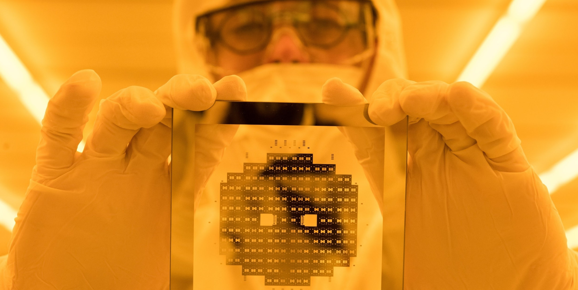
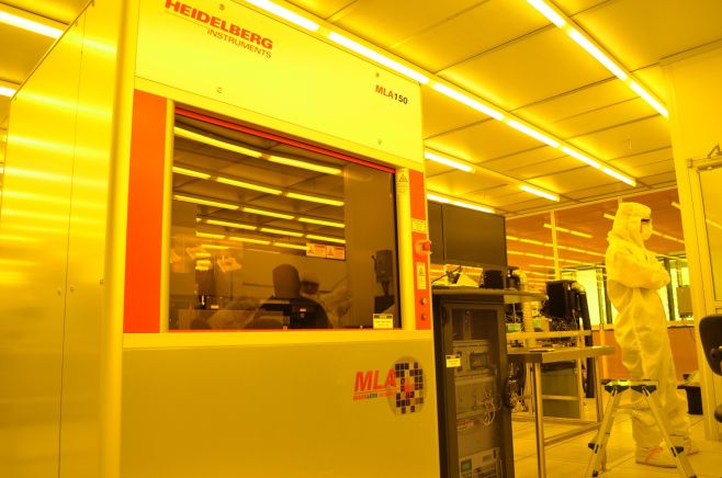
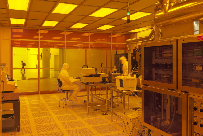
IEN operates and supports the region’s most extensive core research laboratories in several campus buildings. Hands-on, shared user cleanroom space totals 28,500 square feet in the Marcus and Pettit buildings. These cleanrooms are general use for electronics, MEMS, photonics, and materials research, along with a specialized class 100 bays for work at the interface between fabrication and life sciences. Additional laboratories under IEN administration include the Laser Machining Lab, for micro-machining of diverse materials (polymers, glasses, ceramics, metals, and organics) using UV and IR laser sources, and a Teaching Cleanroom dedicated to support advanced training and lab courses taught in the areas of CMOS fabrication, MEMS, and micro/nanoelectronic processing.
Bio Cleanroom
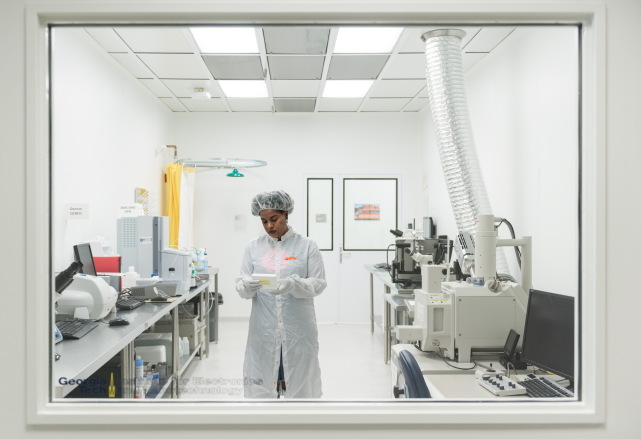
The mission of the Georgia Tech Biocleanroom is to provide the world-class scientific infrastructure to researchers from academia, industry, and government agencies at an affordable rate. The Biocleanroom is one of the major and unique infrastructures in Institute of Electronics and Nanotechnology (IEN) and has been in service since 2009.
The Biocleanroom is a combination of class 1000 cleanroom and bio-safety level II lab. This unique combination has become a desirable environment for contamination-free bio-related fabrication and manufacture. The facility and staff can also assist you in your printing and fabrication, materials characterization, and microscopy needs.
Materials Characterization
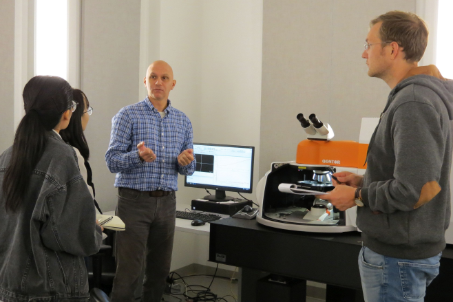
The IEN/IMat Materials Characterization Facility (MCF) is the core facility for materials analysis at Georgia Tech. Its laboratories include the microanalysis suite in the Marcus Nanotechnology Building, one of the most advanced facilities of its kind in the nation.
Available to academic, industry, and government users, the MCF at Georgia Tech is a merger of several labs on campus under one umbrella with a uniform set of fees and policies. The MCF offers a wide variety of microscopy and characterization tools as well as skilled research staff to support your research needs.
SENIC @ JSNN Cleanroom
In collaboration with Georgia Tech IEN, JSNN is an integral partner of the National Nanotechnology Coordinated Infrastructure (NNCI) supported by the National Science Foundation (NSF).
JSNN Core Facilities provides 24/7 open access to laboratories, tools and support for nano and microscale lithography, fabrication, synthesis, characterization, design, and computation, as well as hands-on training in a shared user environment. The fee-for-use based resources, tools, and labs are available to academic, industry, and government users. In addition to the labs and tools, users have access to highly skilled staff and world-class specialized training.
Assembly & Environmental Testing
Located within the Pettit building at Georgia Tech, the Packaging Research Center Assembly and Environmental Testing facility supports interconnect research including wire bonding, flip chip bonding, screen printing and reflow soldering. To ensure a contamination free space, chip assembly and screen-printing capabilities are in a class 1000 bay. The environmental testing facility consists of extended testing in chambers for thermal shock, thermal cycling, and high temperature storage. These processes can all accept device under test measurement or voltage / current application during testing.
High Frequency Testing
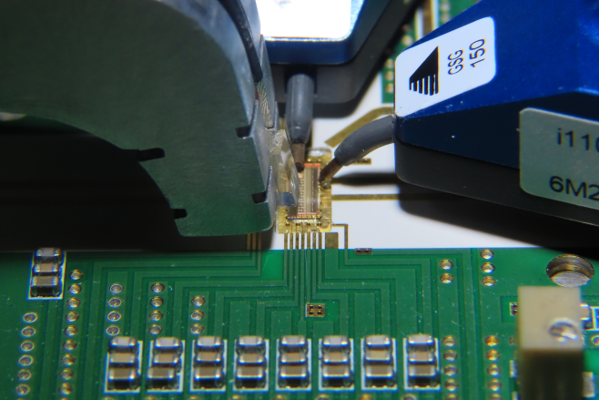
Industry partners working with GEDC faculty and students engage in directed research and collaborate directly with our faculty and students and may establish design centers in Technology Square or within our own center. Support from the Executive Vice President for Research and from our industry partners allows us to create and maintain state-of-the-art laboratory resources, including comprehensive device, circuit and system testing to 300 GHz, the Agilent EE suite of design tools, and a terabit optical networking test bed.

