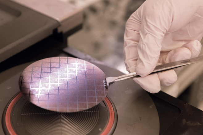
The IEN Instructional Laboratory supports courses for Georgia Tech students that combine lecture and hands-on fabrication experience. Both undergraduate and graduate students gain valuable real-world relevant experience with advanced tool availability, laboratory, and cleanroom environments.
IEN provides support to Georgia Tech colleges and schools for disciplinary and inter-disciplinary courses in microelectronics devices and microelectronics packaging. These hands-on courses, some of which are conducted in world-class prototype cleanroom laboratories, offer students the opportunity to experience complete process cycles from design to fabrication. With approximately 150 enrolled students each year, IEN also provides the staff expertise to run the laboratory sections of the courses in its Teaching Cleanroom.

Integrated Circuit Fabrication - ECE 4452
Introduction to microelectronic processing technologies and CMOS. A course in which students get the opportunity to learn about and experience the manufacturing technologies associated with integrated circuit fabrication. Ultimately the students fabricate basic integrated circuit elements (NMOS, PMOS, capacitors, resistors) as well as more complex CMOS circuits such as ring oscillators, inverters, NAND gates, and NOR gates. The course culminates in the characterization of the fabricated devices and circuits as well as a process design project aimed at improving the existing manufacturing process..

The Science and Engineering of Microelectronic Fabrication - ChBE 4050/6050
A course for senior level undergraduates in ChBE (or Chemistry) and graduate students in the chemical sciences interested in semiconductor materials and fabrication. The course presents the fundamentals and applications of materials and processes used in the fabrication of semiconductor devices, including integrated circuits. The chemical and engineering issues associated with the processing of the materials used in the fabrication of microelectronic devices are covered. The course will have five hands-on laboratory experiments which form the basic unit operations used in semiconductor microfabrication. The course will provide the fundamentals of materials synthesis, chemical and mechanical properties, and chemical reactions. In addition, the sequence of processes used to fabricate metal-oxide semiconductor (MOS) integrated circuits will be presented. The set of exploratory experiments includes silicon dioxide deposition, photolithography, diffusion and semiconductor doping, metallization and silicide formation, and integrated circuit testing. Credit will not be awarded for both CHBE 6050 and CHBE 4050.

Introduction to MEMS - ME/ChBE/ECE 6229
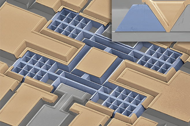
Introduction to Micro-Electro-Mechanical Systems: We designed this course to span all of engineering to explore the theory and practice of MEMS (micro electrical mechanical systems) fabrication, which integrates hands-on learning with the classroom. Graduate students learn the fundamentals of engineering on the microscale while concurrently utilizing the Institute for Electronics and Nanotechnology Cleanroom throughout a 9 laboratory set to create microresonator sensors. Students have stated that the intellectual foundation of the classroom and the hands-on skills learned in the cleanroom were the best aspects of the course. Credit not allowed for both ECE 6229 and ME 6229 or CHBE 6229.

Instructional Lab Coordinator
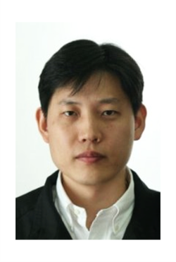
Seung-Joon Paik received his B.S. degree at the School of Electrical Engineering in 1999 and the M.S. and Ph.D. degrees at the Electrical Engineering and Computer Science from Seoul National University, Seoul, Korea, in 2001 and 2005, respectively. His doctorate research focused on the design, microfabrication and testing of silicon microneedles for neurophysiologic applications, including microfluidic channels and microelectrodes. He was with Automation and Systems Research Institute in Seoul National University, as a postdoctoral associate from 2005 to 2007, where he developed sensors and systems of Inertial Measurement Unit (IMU) for localization and locomotion of robots. After joining a spin-off company from the research lab, SML Electronics, Inc., in 2007, he led the process team for the 8-inch wafer-level packaging process and foundry manufacturing process of MEMS accelerometers and gyroscopes for mobile applications as a senior research engineer. In 2008, he joined the MicroSensors and MicroActuators Laboratory (MSMA Lab.) in Georgia Institute of Technology, Atlanta, Georgia. He has led the BioMEMS research group at the MSMA Lab as a postdoctoral fellow. The BioMEMS research group is dedicated to developing micro/nano needles and biosensors for drug delivery and electrochemical sensing. In 2013, as a research engineer II at the Institute for Electronics and Nanotechnology (IEN) in Georgia Tech, he oversees and coordinates lab sections for College of Engineering courses within IEN which provides instructions to students about CMOS transistor fabrication and MEMS fabrication. He has been teaching and mentoring junior-level research engineers and graduate students on design, analysis, micromachining processes, and technical writing and presentation at Seoul National University, SML Electronics, and Georgia Institute of Technology. In 2014, he also worked in Southern Polytechnic State University (currently, Kennesaw State University) as an adjunct professor and taught a course of Microelectronic Engineering and its labs.
He has published 65+ reviewed journal and conference papers, and invented 13+ patents in USA and Korea, and has been a reviewer for the following Journals – IEEE Journal of Microelectromechanical Systems (JMEMS); IOP Journals of Micromechanics and Microengineering, Nanotechnology, Material Science and Technology, Journal of Physics D, and Smart Materials and Structures; and Sensors and Actuators A: Physics. His current interests are in research and development for the micromachining of silicon and polymer materials and in biomedical applications of micromachined devices and also in inertial sensors, 3-D multi-chip packaging of MEMS devices, energy storage/conversion devices and nano-scale structures.
Seung-Joon Paik, Ph.D.
Research Engineer II
Instructional lab coordinator
seung.paik@ien.gatech.edu
Phone: 404-894-8807
Office: Pettit 205


